Strain Gage Conditioner
Schematic
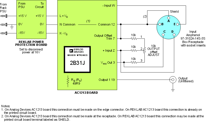
The above block diagram is available in the original CorelDRAW 9 format and in PDF.
List of components:
- 2B31J Strain Gage/RTD Conditioner (Word Doc Format, PDF format)
- Parts List (Excel)
Note: It is suspected that there is a documentation error in the spec sheets for 2B31J. Tests reveal a sign reversal at the output of the In Amp. It would appear that the W and Z inputs should be interchanged. Also, the equation for gain (G) is experimentally correct but does not agree in sign based on the schematic of the signal conditioner.
Functional Description
 faceplate.cdr: CorelDRAW 9 file used to make
faceplates
faceplate.cdr: CorelDRAW 9 file used to make
faceplates
This module is a Wheatstone bridge amplifier. It is used to amplify the output voltage of a torque transducer or load cell connected via the input receptacle. The module is based on a 2B31J strain gage conditioner. This conditioner contains all the necessary circuitry to excite a bridge and measure its output; it contains an instrumentation amplifier (In Amp), low-pass filter (unused in our applications), an adjustable transducer excitation source, among other things.
The gain, G, of the module is set as follows:
G=(1+94k ohm / Rg)*(20k ohm / (Rf+16.2k ohm))
where Rf is a fine span adjustable resistor inside the module with a max of 10 kohm and Rg is 50 ohms. (The standard in the lab is to have a gain of approximately 2000.)
The offset of the input signal can be adjusted by varying the Offset trim pot accessible from the front panel. This would be used to, say, compensate for unbalance in the bridge transducer or to apply a bias on the output. (The available offset range depends on the resistance of the bridge connected to the module.) It is important to keep in mind that to minimize output drift this adjustment should NOT be used to null the input offset voltage inherent to the In Amp.
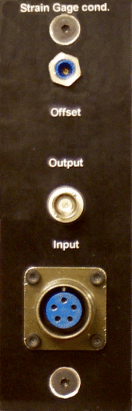
 Input offset voltage
should be independently nulled using the INPUT OFFSET TRIM potentiometer
located on the printed circuit board, inside the module, with the In Amp
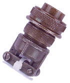
inputs shorted to common. For this procedure use the input terminator
shown to the left.
Input offset voltage
should be independently nulled using the INPUT OFFSET TRIM potentiometer
located on the printed circuit board, inside the module, with the In Amp
inputs shorted to common. For this procedure use the input terminator
shown to the left.
Testing the Module
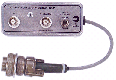 The differential
voltage driving this module is typically in the low mV range. Function
generators in the lab are not able to produce signals of this amplitude.
The tester box shown to the left scales down the input signal (at the
In BNC connector) by approximately 1000, making signal levels compatible
with the module.
The differential
voltage driving this module is typically in the low mV range. Function
generators in the lab are not able to produce signals of this amplitude.
The tester box shown to the left scales down the input signal (at the
In BNC connector) by approximately 1000, making signal levels compatible
with the module.
The layout of the box may be found in this
Corel DRAW 9 file.
The schematic diagram of the tester along with design equations are shown
below.
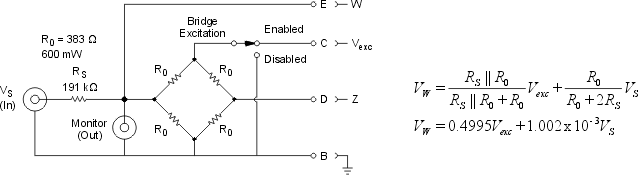
The tester is a Wheatstone bridge onto which a perturbation may be applied as Vs. The bridge portion of the circuitry is necessary so that a differential input is presented to the module. (Otherwise the module tends to saturate and the output offset adjust does not function properly.)
The non-inverting input of the module is affected by the output offset adjust circuitry. In order to simplify the tester box design equations the perturbation (or test) signal is applied to the module's inverting input; pin E of the input receptacle. Though this isolates the voltage divider circuitry from the offset circuitry it also introduces a 180-deg phase shift in all responses which may have to be taken into account.
The Bridge Excitation toggle switch is set to Enabled during module testing. When the switch is in the Disabled position the bridge excitation voltage is set to zero allowing one to monitor the actual test signal driving the module on a dc-coupled oscilloscope. This setting may also be used to determine the actual voltage divider ratio (in Vw).
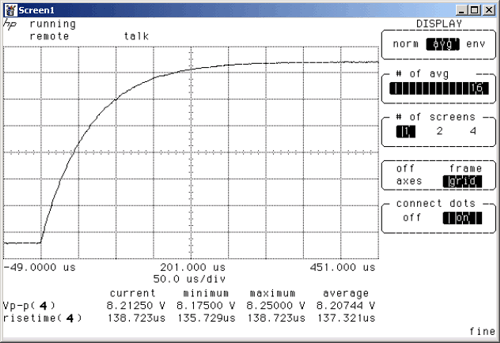
Step Response
The typical step response of a module set to a gain of 2000 is shown below. The 10-90% risetime is ~137 us. (16 averages were used.)
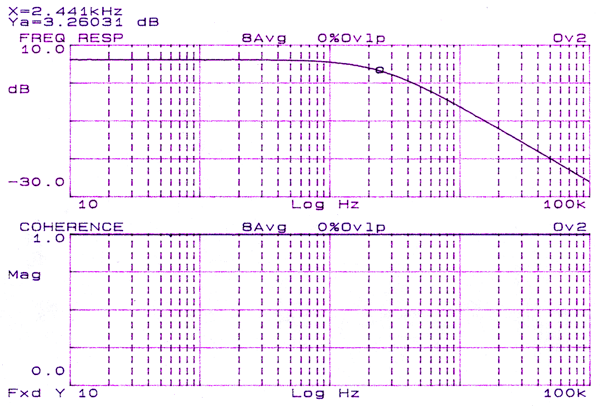
Frequency Response
The frequency response of this module is shown below and was measured using an HP dymanic signal analyzer (random excitation signal, 1Vpk.) The true gain is 60dB higher owing to the fact that the testing box (see above) attenuates the input signal by 1000. Hence, the apparent pass band gain of 6.2 dB actually corresponds to a gain of 66.2dB (or approximately 2000.) The cutoff frequency, indicated by the circle, is around 2.4 kHz and the roll-off is -20dB/decade. The coherence function is relatively flat, showing small dips at 60 Hz and 180 Hz.
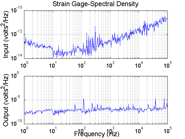
Noise Analysis
The output to 0 volt noise is as follows:
Output Offset Adjust Circuitry
To understand the operation of the level shifting circuit consider the
equivalent circuit shown here, depicting a bridge connected to the module
and the input stage of the 2B31J conditioner. For simplicity, assume an
ideal In Amp and let the bridge be balanced with resistance 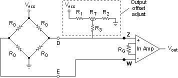 R0
for each arm. When the bottom of R3 is not connected to the right half
of the bridge each In Amp input, Z and W, sees Vexc/2 volts and produces
Vout = 0V. Connecting R3 to the bridge creates another voltage divider
network between the right side of the bridge and the output offset adjust
circuitry. The resulting voltage at Z is given as follows,
R0
for each arm. When the bottom of R3 is not connected to the right half
of the bridge each In Amp input, Z and W, sees Vexc/2 volts and produces
Vout = 0V. Connecting R3 to the bridge creates another voltage divider
network between the right side of the bridge and the output offset adjust
circuitry. The resulting voltage at Z is given as follows,
Parameter a represents the fractional displacement of RT's wiper.
By setting R1 = R2, at mid-point wiper position (a = 0.5) along
RT the voltage at the wiper is Vexc/2. In this case the offset-adjust
circuitry has no effect on the baseline voltage at Z since the voltages
at each terminal of R3 are identical (so no current flows through the
component.) The In Amp output is still 0V. However, moving RT's wiper
to the left (a -> 1) raises the voltage at Z above Vexc/2 causing
the In Amp output to swing positively. Conversely, moving RT's wiper to
the right (a -> 0) lowers the voltage at Z below Vexc/2 causing
the In Amp output to swing negatively. Effectively, because a bridge produces
a differential output centered about half of the excitation voltage, a
unipolar output offset adjusting circuit is able to produce bipolar offset
at Vout.
Use this MATLAB M-file to evaluate
the range of Vz for various component values.
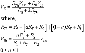
Printed Circuit Board
Click on the image for larger view.
Cick here for an image
of the PCB in PDF format.
Click here for the PCB source file and associated
application. (Zip file 6.41MB)
Faceplate CAM File
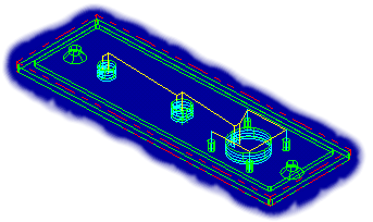 The
component mounting holes may be machined on a prepared faceplate
base using this Mastercam X file. (379 KB)
The
component mounting holes may be machined on a prepared faceplate
base using this Mastercam X file. (379 KB)
Last Modified: 2007-04-10 Ross Wagner